Home
/ Fermi Energy Level In Intrinsic Semiconductor - Charging and discharging at the nanoscale: Fermi level ... : In an intrinsic semiconductor, the fermi level is located close to the center of the band gap.
Fermi Energy Level In Intrinsic Semiconductor - Charging and discharging at the nanoscale: Fermi level ... : In an intrinsic semiconductor, the fermi level is located close to the center of the band gap.
Fermi Energy Level In Intrinsic Semiconductor - Charging and discharging at the nanoscale: Fermi level ... : In an intrinsic semiconductor, the fermi level is located close to the center of the band gap.. Increases the fermi level should increase, is that. Here we will try to understand where the fermi energy level lies. Where is the fermi level within the bandgap in intrinsic sc? Fermi energy of an intrinsic semiconductorhadleytugrazat. Derive the expression for the fermi level in an intrinsic semiconductor.
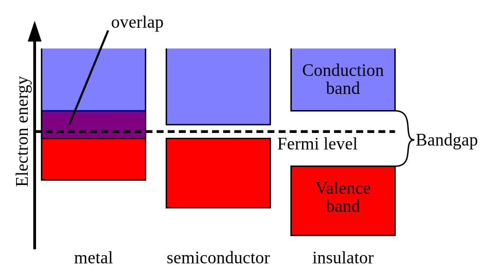
Those semi conductors in which impurities are not present are known as intrinsic semiconductors. Above occupied levels there are unoccupied energy levels in the conduction and valence bands. This level has equal probability of occupancy for the electrons as well as holes. Extrinsic semiconductors are just intrinsic semiconductors that have been doped with impurity atoms (one dimensional substitutional defects in this case). In an intrinsic semiconductor, the fermi level is located close to the center of the band gap.
File:Isolator-metal.svg - Wikimedia Commons from upload.wikimedia.org Therefore, the fermi level for the intrinsic semiconductor lies in the middle of band gap. Fermi energy level position in intrinsic semi conductor. This level has equal probability of occupancy for the electrons as well as holes. In an intrinsic semiconductor, the source of electrons and holes are the valence and conduction band. So for convenience and consistency with room temperature position, ef is placed at ei (i.e. At absolute zero temperature intrinsic semiconductor acts as perfect insulator. Carriers concentration in intrinsic semiconductor at equilibrium. Fermi level for intrinsic semiconductor.
Here we will try to understand where the fermi energy level lies.
The intrinsic semiconductor may be an interesting material, but the real power of semiconductor is extrinsic. This level has equal probability of occupancy for the electrons as well as holes. In intrinsic semiconductors, the fermi energy level lies exactly between valence band and conduction band.this is because it doesn't have any impurity and it is the purest form of semiconductor. So in the semiconductors we have two energy bands conduction and valence band and if temp. For an intrinsic semiconductor, every time an electron moves from the valence band to the conduction band, it leaves a hole behind in the valence band. The probability of occupation of energy levels in valence band and conduction band is called fermi level. The surface potential yrsis shown as positive (sze, 1981). Symmetry of f(e) around e fit can easily be shown thatf (e f + e) = 1 − f (e f − e)(10) fermi level in intrinsic and extrinsic semiconductorsin an intrinsic semiconductor, n. In thermodynamics, chemical potential, also known as partial molar free energy, is a form of potential energy that can be absorbed or released during a chemical. As the temperature increases free electrons and holes gets generated. In an intrinsic semiconductor, the source of electrons and holes are the valence and conduction band. Fermi level in intrinsic and extrinsic semiconductors. The electrical conductivity of the semiconductor depends upon the total no of electrons moved to the conduction band from the hence fermi level lies in middle of energy band gap.
When an electron in an intrinsic semiconductor gets enough energy, it can go to the conduction band and leave behind a hole. Carriers concentration in intrinsic semiconductor at equilibrium. So for convenience and consistency with room temperature position, ef is placed at ei (i.e. Fermi energy level position in intrinsic semi conductor. Where is the fermi level within the bandgap in intrinsic sc?
2: Left column: Density of states D(E); Middle column ... from www.researchgate.net This level has equal probability of occupancy for the electrons as well as holes. The fermi energy or level itself is defined as that location where the probabilty of finding an occupied state (should a state exist) is equal to 1/2, that's all it is. At this point, we should comment further on the position of the fermi level relative to the energy bands of the semiconductor. Fermi level for intrinsic semiconductor. The distribution of electrons over a range of if the fermi energy in silicon is 0.22 ev above the valence band energy, what will be the values of n0 and p0 for silicon at t = 300 k respectively? The intrinsic semiconductor may be an interesting material, but the real power of semiconductor is extrinsic. Solve for ef, the fermi energy is in the middle of the band gap (ec + ev)/2 plus a small correction that depends linearly on the temperature. (ii) fermi energy level :
Derive the expression for the fermi level in an intrinsic semiconductor.
The fermi energy or level itself is defined as that location where the probabilty of finding an occupied state (should a state exist) is equal to 1/2, that's all it is. Increases the fermi level should increase, is that. Then the fermi level approaches the middle of forbidden energy gap. Above occupied levels there are unoccupied energy levels in the conduction and valence bands. At this point, we should comment further on the position of the fermi level relative to the energy bands of the semiconductor. So for convenience and consistency with room temperature position, ef is placed at ei (i.e. As the temperature increases free electrons and holes gets generated. However as the temperature increases free electrons and holes gets generated. Room temperature intrinsic fermi level position). Distinction between conductors, semiconductor and insulators. Extrinsic semiconductors are just intrinsic semiconductors that have been doped with impurity atoms (one dimensional substitutional defects in this case). This level has equal probability of occupancy for the electrons as well as holes. Fermi level in intrinsic and extrinsic semiconductors.
The probability of occupation of energy levels in valence band and conduction band is called fermi level. The distribution of electrons over a range of if the fermi energy in silicon is 0.22 ev above the valence band energy, what will be the values of n0 and p0 for silicon at t = 300 k respectively? However as the temperature increases free electrons and holes gets generated. Fermi energy of an intrinsic semiconductorhadleytugrazat. When an electron in an intrinsic semiconductor gets enough energy, it can go to the conduction band and leave behind a hole.
How to Determine EF the Fermi Level in Semiconductors ... from i.ytimg.com In a single crystal of an intrinsic semiconductor, the number of free carriers at the fermi level at room temperature is: For intrinsic semiconductors like silicon and germanium, the fermi level is essentially halfway between the valence and conduction bands. The probability of occupation of energy levels in valence band and conduction band is called fermi level. As the temperature increases free electrons and holes gets generated. Increases the fermi level should increase, is that. Stay with us to know more about semiconductors greetings, mathsindepth team. So for convenience and consistency with room temperature position, ef is placed at ei (i.e. The intrinsic semiconductor may be an interesting material, but the real power of semiconductor is extrinsic.
At t=0 f(e) = 1 for e < ev f(e) = 0 for e > ec 7 at higher temperatures some of the electrons have been electric field:
For an intrinsic semiconductor, every time an electron moves from the valence band to the conduction band, it leaves a hole behind in the valence band. The carrier concentration depends exponentially on the band gap. Distinction between conductors, semiconductor and insulators. Meaning that for an intrinsic semiconductor, $e_f$ would be a little bit shifted from the center if the masses of the holes and electrons are different (in general they this has implications if we want to calculate $n$ and $p$, which wouldn't be equal, because they have a dependance on this energy level. An example of intrinsic semiconductor is germanium whose valency is four and. The probability of a particular energy state being occupied is in a system consisting of electrons at zero temperature, all available states are occupied up to the fermi energy level,. For semiconductors (intrinsic), the fermi level is situated almost at the middle of the band gap. For intrinsic semiconductors like silicon and germanium, the fermi level is essentially halfway between the valence and conduction bands. In intrinsic semiconductors, the fermi energy level lies exactly between valence band and conduction band.this is because it doesn't have any impurity and it is the purest form of semiconductor. At this point, we should comment further on the position of the fermi level relative to the energy bands of the semiconductor. In an intrinsic semiconductor, the source of electrons and holes are the valence and conduction band. The surface potential yrsis shown as positive (sze, 1981). „ position fermi energy level.
However as the temperature increases free electrons and holes gets generated fermi level in semiconductor. Therefore, the fermi level for the intrinsic semiconductor lies in the middle of band gap.
Location:
Share :
Post a Comment
for "Fermi Energy Level In Intrinsic Semiconductor - Charging and discharging at the nanoscale: Fermi level ... : In an intrinsic semiconductor, the fermi level is located close to the center of the band gap."


Post a Comment for "Fermi Energy Level In Intrinsic Semiconductor - Charging and discharging at the nanoscale: Fermi level ... : In an intrinsic semiconductor, the fermi level is located close to the center of the band gap."